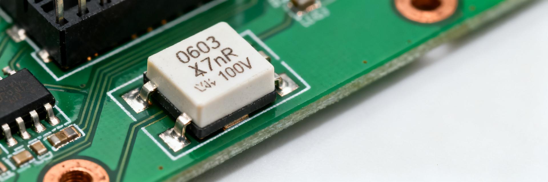
Point: For precision RF and timing work, the 220pF C0G part is chosen for minimal drift and loss. Evidence: Typical C0G/NP0 dielectrics specify near 0 ±30 ppm/°C and stable capacitance across a wide commercial range; rated voltages commonly appear at 16–50 V on component tables. Explanation: That stability reduces retune cycles and failure risk in oscillators and filters, and specific part numbers such as GMT10CG221J50NT4 are often cross-checked against datasheet tables for exact VR and DF values.
Point: This note translates datasheet figures into actionable PCB and test guidance. Evidence: Manufacturer tables list capacitance, tolerance, DF/tanδ, SRF, insulation resistance, recommended land pattern and reflow limits. Explanation: Reading those fields consistently lets engineers set derating, inspection limits, and measurement plans that map directly from datasheet insights to reliable board behavior.
1 — What "220pF C0G (NP0) 0603" actually means (background)
Meaning of the code: capacitance, dielectric, and package
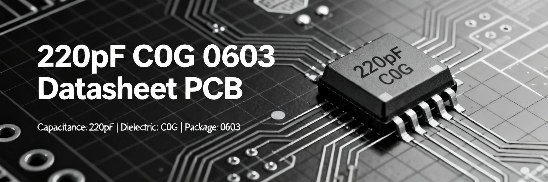
Point: The label encodes capacitance value, dielectric class, and package size. Evidence: "220pF" denotes nominal capacitance with common tolerances ±1% or ±5%; "C0G/NP0" denotes a temperature coefficient ≈0 ±30 ppm/°C; "0603" refers to the imperial footprint (metric 1608) and typical terminations are end‑electrodes compatible with standard SMT solder. Explanation: Understanding these tokens lets you read a datasheet quickly—tolerance column, tempco row, and mechanical drawing give the designer the primary selection cues for precision circuits.
Typical application contexts
Point: 220pF C0G 0603 parts are standard in high‑stability, low‑loss networks. Evidence: Datasheet application notes and typical‑use tables show usage in RF matching networks, high‑Q filters, timing networks, charge pump loops, and decoupling on sensitive analog nodes. Explanation: The near‑zero temperature coefficient and low dissipation factor minimize phase and amplitude drift, making the 0603 capacitor a compact choice where space and stability matter.
2 — Key electrical specs to extract from the datasheet (data analysis)
Core electrical parameters and how to read them
Point: Key table fields to record are capacitance/tolerance, rated voltage, tempco, DF/tanδ, insulation resistance, DC bias characteristics, and SRF. Evidence: Typical datasheet columns present C (pF), tolerance (%), VR (V), tempco (ppm/°C), DF at specific test freq, IR (MΩ), and SRF (MHz). Explanation: Capture these entries into a selection checklist so you can compare parts quantitatively: DF and SRF indicate usable frequency band, VR and bias curves inform derating, and IR/withstand data feed qualification limits.
Performance under stress: DC bias, frequency, and temperature effects
Point: Even C0G parts have measurable behavior versus bias, frequency, and temperature. Evidence: Datasheets often show DC‑bias curves (small percent change for C0G vs. larger shifts for X7R), DF vs. frequency traces, and tempco charts converting ppm/°C into percent change across the operating range. Explanation: Use those figures to confirm that at your operating DC and RF frequency the part remains within required tolerance and Q—SRF indicates where series resonance will limit capacitance effectiveness.
3 — Mechanical & reliability specs: what matters for assembly and lifetime (data + method)
Package, mechanical strength, and soldering constraints
Point: Mechanical and assembly notes prevent failures like cracking and tombstoning. Evidence: Datasheets include recommended land patterns, maximum reflow profiles (peak temp and time above liquidus) and moisture sensitivity level (MSL) data. Explanation: Follow the recommended pad geometry, limit solder paste volume, and adhere to reflow limits; for 0603 capacitors, controlled solder fillet and balanced pads reduce mechanical stress during cooling and handling.
Reliability metrics: insulation resistance, dielectric strength, and aging
Point: Reliability fields define acceptance for incoming inspection and lifetime expectations. Evidence: Typical IR values are given in MΩ at a specified test voltage; dielectric withstand tests list test voltage and duration; aging notes for C0G indicate negligible drift compared with high‑K dielectrics. Explanation: Record IR limits and withstand voltage from the datasheet for AQL checks; because C0G shows minimal aging, long‑term capacitance shift is usually dominated by assembly stress or mechanical damage rather than dielectric change.
4 — Selection & design guidelines (method / practical)
Choosing voltage rating and tolerance for reliability
Point: Select VR and tolerance with margin to ensure field reliability. Evidence: Datasheets show rated voltages (commonly 16 V, 25 V, 50 V) and may note capacitance vs. applied DC; higher VR parts sometimes require different stack geometries with altered volumetric capacitance. Explanation: Choose a rated voltage comfortably above expected DC plus transients, and pick tolerance (±1% for timing) that keeps filter or oscillator performance within spec—confirm the datasheet’s DC‑bias table so actual on-board C meets nominal requirements.
PCB placement and layout tips for best performance
Point: Layout determines effective series inductance and stray coupling. Evidence: Practical guidance from datasheets and application notes emphasizes short traces, direct ground reference, and proximity to active nets. Explanation: Place the 0603 capacitor with the shortest possible trace to the node and maintain a low‑impedance return; add thermal/mechanical relief where appropriate to reduce stress and improve measurement repeatability.
5 — Testing, measurement & verification (case / action)
Recommended measurement methods and pitfalls
Point: Accurate measurement of 220pF C0G requires correct fixturing and settings. Evidence: Datasheet test conditions list test frequency, test voltage and fixture compensation requirements; LCR measurement at multiple frequencies plus open/short compensation is typical. Explanation: Use low‑inductance fixtures, match test frequency to your application band, and beware of test‑voltage‑induced bias; record DF/tanδ at the intended operating frequency per the datasheet insights.
Pass/fail criteria and field verification
Point: Define inspection limits from datasheet numbers for incoming and field testing. Evidence: Datasheets provide tolerance, DF limits, IR minima, and environmental test conditions (thermal cycle, humidity). Explanation: Create sample plans that reference those values—e.g., incoming C within tolerance, DF below stated max at test freq, IR above minimum—then apply environmental stress tests mirroring datasheet conditions to validate long‑term performance.
| Parameter | Datasheet field to record |
|---|---|
| Capacitance & tolerance | C (pF), ±1% or ±5% |
| Rated voltage | VR (V) and DC‑bias curve |
| Tempco | ppm/°C (C0G ≈0 ±30 ppm/°C) |
| Dissipation factor | DF or tanδ at test freq |
| SRF | SRF (MHz) |
| Mechanical | Land pattern, peak reflow temp, MSL |
Summary
- Record capacitance, tolerance, VR, tempco and DF from the manufacturer datasheet to ensure the 220pF C0G part meets circuit stability and RF loss targets.
- Use DC‑bias and SRF data to confirm usable frequency band and on‑board capacitance under operating voltage and avoid surprises in filters and oscillators.
- Follow recommended land patterns and reflow limits for 0603 capacitor assembly to minimize cracking and tombstoning; capture MSL and mechanical notes for procurement and IPC handling.
FAQ
How does DC bias affect a 220pF C0G capacitor?
Point: DC bias produces minimal capacitance shift for C0G materials. Evidence: Datasheet bias curves for C0G show only small percent change versus applied voltage compared with high‑K dielectrics. Explanation: For timing and RF usage, rely on the datasheet bias table to confirm that under expected DC the effective capacitance remains within tolerance; if your design is near tolerance limits, choose a higher nominal value or tighter tolerance.
What test settings should be used to verify DF for a 0603 capacitor?
Point: Match LCR settings to application frequency and use proper compensation. Evidence: Datasheet specifies DF/tanδ at one or more test frequencies and a test voltage; fixture inductance and open/short compensation are typically noted. Explanation: Measure DF at the target operating frequency with a low‑inductance fixture, apply open/short compensation, and use the same test voltage stated on the datasheet to get comparable results.
Which datasheet mechanical fields are critical for PCB assembly of 0603 parts?
Point: Land pattern, peak reflow temperature, and MSL drive assembly success. Evidence: Manufacturer mechanical drawings list recommended land pattern and reflow profile; MSL indicates floor life restrictions after baking. Explanation: Implement the recommended pad geometry, control paste volume to avoid tombstoning, and follow MSL/handling notes to prevent moisture‑induced failures during reflow and storage.
Why is the 0603 package size preferred for RF tuning capacitors?
Point: 0603 package layout optimizes Parasitic Inductance (ESL). Evidence: High-frequency application notes show smaller imperial footprints exhibit lower series self-inductance. Explanation: Utilizing the 0603 scale minimizes RF path length and matches SMT component dimensions to optimal microstrip trace widths, suppressing parasitic effects up to high-gigahertz limits.